
Roll over image to zoom in
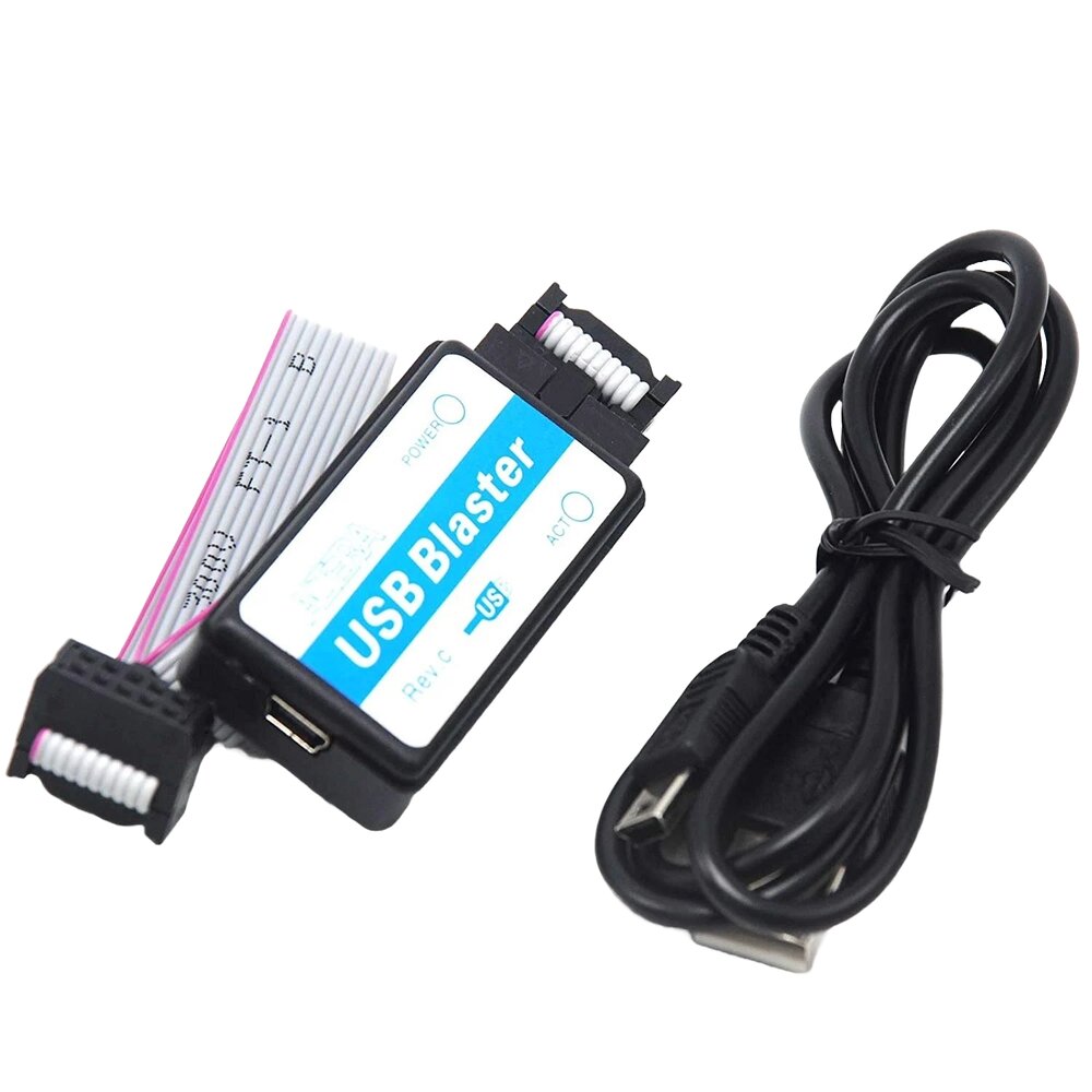
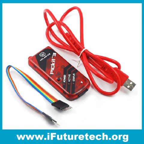
USB Blaster ALTERA CPLD/FPGA Programmer
₹249.00
The USB Blaster is the essential tool for anyone working with Intel (formerly Altera) Field Programmable Gate Arrays (FPGAs) and Complex Programmable Logic Devices (CPLDs). This compact, high-speed programming unit seamlessly bridges your computer’s USB port and the target device’s JTAG, AS (Active Serial), or PS (Passive Serial) configuration headers. Engineers and students rely on the USB Blaster for quickly and reliably downloading configuration data, enabling in-system programming (ISP), and performing invaluable real-time debugging directly from the Quartus Prime software. It’s an indispensable link in the development chain, simplifying the process of bringing complex digital designs from concept to silicon.
Key Features:
- Broad Device Support: Program and configure virtually all Altera (Intel) FPGA families, including Cyclone, Stratix, Arria, and MAX series CPLDs.
- Multiple Configuration Modes: Supports JTAG, Active Serial (AS), and Passive Serial (PS) modes, giving you the flexibility to program various memory and configuration devices.
- High-Speed USB 2.0 Interface: Ensures fast and efficient data transfer from your PC to the target device, dramatically reducing programming time.
- Seamless Software Integration: Works directly with the Intel Quartus Prime development software, providing a unified environment for design, compilation, and programming.
- Adjustable Voltage Support: The programmer’s output voltage adjusts automatically to the target board’s voltage (typically supporting 1.5V to 5.0V), eliminating the need for external level shifters.
- In-System Debugging: Facilitates real-time signal monitoring and debugging using embedded logic analyzers like SignalTap II, a critical feature for complex designs.
Technical Specifications:
- Interface Type: USB 2.0
- Target Voltage Support: 1.5V to 5.0V DC (Auto-sensing)
- Supported Protocols: JTAG, AS (Active Serial), PS (Passive Serial)
- Supported Operating Systems: Windows, Linux, and macOS (with appropriate drivers)
- Target Connector: Standard 10-pin JTAG/AS header (2×5 pin connector)
- Data Transfer Rate: Up to 6 Mbit/s (protocol dependent)
Mechanical Specifications:
- Enclosure: Compact plastic or metal casing for durability and portability.
- LED Indicators: Status LEDs typically indicate power, USB connectivity, and target connectivity/activity.
- Connector: Standard USB-B or Mini-USB port for PC connection.
- Material: Durable PCB enclosed in a protective shell.
Dimensions:
- Length: ~70 mm
- Width: ~45 mm
- Height: ~20 mm
Pinout and Wiring:
- TDO (Test Data Out): Data from the target device to the programmer (JTAG).
- TDI (Test Data In): Data from the programmer to the target device (JTAG).
- TCK (Test Clock): Clock signal for synchronous data transfer (JTAG).
- TMS (Test Mode Select): Controls the JTAG state machine.
- VCC/VTGT (Target Voltage): Senses the target board’s operating voltage.
- GND (Ground): Common ground connection.
- ASDO/nCE (Active Serial Data Out/Chip Enable): Used for Active Serial mode programming.
- Wiring Note: Connect the 10-pin flat ribbon cable from the USB Blaster to the JTAG/AS header on your target FPGA/CPLD board, ensuring Pin 1 alignment. The programmer senses the target’s voltage through the VTGT pin.
Datasheet Reference:
- Download USB Blaster User Guide (Intel/Altera)
Commonly Used in:
- Digital Design Labs: Essential for educational institutions teaching hardware description languages (VHDL/Verilog) and FPGA development.
- Embedded System Prototyping: Key tool for engineers validating logic and peripherals on custom PCB designs.
- Commercial Product Development: Used in the production testing and initial programming of devices incorporating Intel (Altera) logic.
Applications:
- Device Configuration: Downloading compiled configuration files (e.g., .sof, .pof) to the FPGA/CPLD or external configuration memories.
- System Debugging: Monitoring internal signals and optimizing timing with SignalTap II logic analyzer.
- In-System Programming (ISP): Updating firmware or configuration data on devices already soldered onto a PCB.
Equivalent Models:
- Platform Cable USB (Xilinx): The comparable programmer for Xilinx FPGAs.
- J-Link (SEGGER): Primarily for microcontrollers, but some advanced versions offer JTAG support for general devices.
- ByteBlaster II (Legacy Altera): An older, parallel-port-based Altera programmer.
Package Includes:
- 1 x USB Blaster ALTERA CPLD/FPGA Programmer
- 1 x 10-Pin JTAG/AS Programming Cable
- 1 x USB Type-A to Type-B Cable (or Mini-USB Cable)
Additional information
| Weight | 50 g |
|---|

Reviews
There are no reviews yet.