
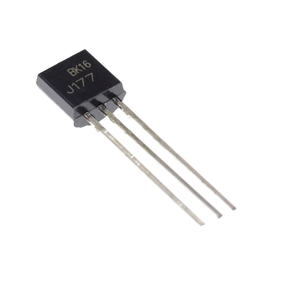
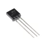
J177 P-Channel Silicon Field-effect Transistor TO-92
₹65.00
J177 P-Channel Silicon Field-effect Transistor TO-92 is a reliable JFET (Junction Field-Effect Transistor) specifically designed for applications requiring high input impedance and low-noise amplification. This P-channel device operates in the depletion mode, offering excellent performance as a switch or as a constant current source. Consequently, design engineers frequently select the J177 for sensitive pre-amplifier circuits and analog signal conditioning stages where minimal signal degradation is critical. Furthermore, its small, through-hole TO-92 package makes it easy to integrate into conventional printed circuit boards, delivering a cost-effective solution for precision instrumentation. The J177’s ability to handle small analog signals with high fidelity ensures stable operation across a wide range of operating conditions.
Key Features:
- P-Channel JFET: This P-channel configuration offers unique biasing flexibility, complementing N-channel devices in analog circuit design.
- High Input Impedance: Provides extremely high resistance at the gate terminal, minimizing loading effects on sensitive signal sources and improving circuit efficiency.
- Low Noise Characteristics: Engineered for minimal thermal and flicker noise, making it ideal for use in high-gain audio and instrumentation pre-amplifiers.
- Low Leakage Current: Maintains exceptionally low gate leakage (IGSS), ensuring stability and high accuracy in precise current measurements and integration circuits.
- TO-92 Package: The ubiquitous, compact TO-92 plastic package supports easy manual or automated insertion into standard through-hole PCB designs.
Technical Specifications:
- Transistor Type: P-Channel JFET (Depletion Mode)
- Drain-Source Voltage (VDS): −30 V maximum
- Gate-Source Voltage (VGS): +30 V maximum
- Gate-Source Cut-off Voltage (VGS(off)): Typically 1.0 V to 6.0 V
- Drain Current (ID): 10 mA maximum continuous
- Gate Reverse Current (IGSS): 1.0 nA maximum at 25°C
- Power Dissipation (PD): 625 mW maximum
- Operating Junction Temperature (TJ): −55°C to +150°C
Mechanical Specifications:
- Package Style: TO-92 (Radial, Through-Hole)
- Body Material: Plastic (Epoxy)
- Lead Finish: Sn-Pb or 100% Sn (check specific batch)
- Moisture Sensitivity Level (MSL): MSL 1 (Unlimited floor life at ≤30°C/85% RH)
Dimensions:
- Body Height (H): ≈ 4.6 mm
- Body Diameter (Φ): ≈ 4.8 mm
- Lead Pitch (E): 1.27 mm (Standard TO-92 center-to-center)
- Overall Lead Length (L): ≈ 14.0 mm
- Weight: ≈ 0.2 g (Extremely light)
Pinout and Wiring:
- Pin 1 (Source – S): Connects to the common reference point or where current exits the channel.
- Pin 2 (Gate – G): Connects to the input control voltage terminal; controls the current flow between the Source and Drain.
- Pin 3 (Drain – D): Connects to the negative supply terminal or where current enters the channel in a P-channel device.
- Wiring Note: Always orient the flat side of the TO-92 package toward you to correctly identify the pin order (S-G-D from left to right).
Datasheet Reference:
Commonly Used in:
- Voltage Controlled Resistors (VCRs): Utilizing the VGS vs. RDS(on) characteristic for analog signal control.
- Audio Equipment: Serving as the input stage in high-fidelity audio mixers and pre-amplifiers due to its low noise floor.
- Oscillators: Forming part of the feedback network in stable Colpitts and Hartley oscillator circuits.
Applications:
- High-Impedance Amplifiers: Building the first stage of instrumentation amplifiers to prevent loading of sensors (e.g., pH probes, high-impedance transducers).
- Constant Current Sources (CCS): Using the transistor’s saturation region to create highly stable current mirrors and bias networks.
- Sample and Hold Circuits: Serving as low-leakage analog switches where signal integrity must be maintained during the hold phase.
Equivalent Models:
- 2N5116: A common alternative P-channel JFET with similar characteristics, often used interchangeably in general-purpose circuits.
- J176 / J175: These are variants within the same JFET family, differing primarily in the VGS(off) and IDSS ratings. However, always verify specific parameter match requirements before substitution.
- BF256B: A European-style JFET often found as a functional replacement in linear applications.
Package Includes:
- 1 x J177 P-Channel JFET Transistor TO-92
Additional information
| Weight | 1 g |
|---|
Reviews
There are no reviews yet.